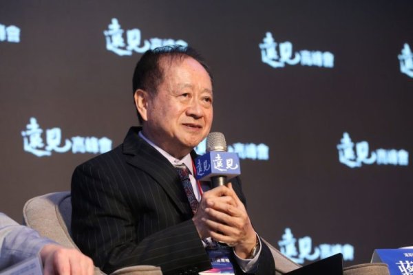
Jiang Shangyi, director of Hon Hai Technology Group, said on the 6th that AI is a new driving force for the future development of semiconductors. From mainframe computers, personal computers, smartphones, to today’s artificial intelligence, each wav...
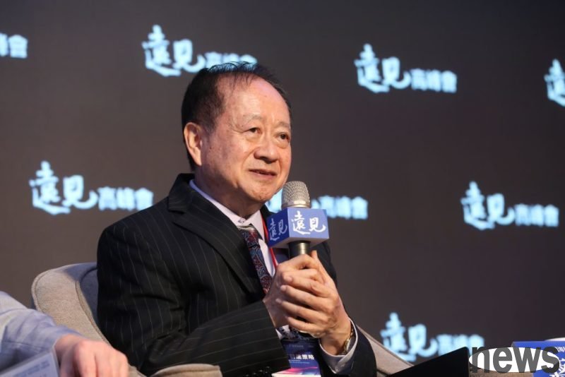
Jiang Shangyi, director of Hon Hai Technology Group, said on the 6th that AI is a new driving force for the future development of semiconductors. From mainframe computers, personal computers, smartphones, to today’s artificial intelligence, each wave of technology has redefined the meaning of Moore’s Law. The difference is that the drivers in the past were all single products. Although the shipment volume was huge, the form was clear and the uses were concentrated. This is not the case with AI. Although AI is still in the infrastructure construction stage and is mainly concentrated in data centers, this is only the first step.
Jiang Shangyi stated at the "2025 Vision Summit" that the development of AI will enter the application stage, that is, from the cloud to the edge (Edge Computing), or some people call it AIoT (Artificial Intelligence Internet of Things). He explained that at this stage, there will be thousands or tens of thousands of different application products, including smart cars, robots, smart homes, smart cities, etc. The diversification of these applications poses new challenges to the design and manufacturing of semiconductors.
However, in the past, process upgrades were mostly focused on a single architecture and high-volume products, but the diversification of AI applications in the future will render the economies of scale of traditional chip design ineffective. He emphasized that the design cost of today's most advanced processes, such as TSMC's sub-5nm products, is approximately US$2 billion. Nowadays, if a design company invests US$200 million in design first, it is not worthwhile at all if the product sales do not reach US$1 billion.
Therefore, he believes that chiplets are the key solution. The concept of chiplets is like building blocks that can be freely combined according to needs. High-computing modules can be reused in different products, which can not only share development costs but also improve market flexibility, becoming the cornerstone of a new architecture in the AI era. However, Moore's Law is approaching physical limits. Jiang Shangyi reminded that when the process shrinkage slows down, even if Taiwan still leads the world in the field of wafer foundry and packaging and testing, its leading edge will be challenged. The future breakthrough may not be in the process, but in packaging.
Jiang Shangyi emphasized that in the past, packaging was only an aid and cost control. Now, with the maturity of advanced packaging technologies such as CoWoS and InFO, the integration efficiency between chips has become the key to improving performance. In addition to maintaining the leadership in semiconductor manufacturing and packaging, Jiang Shangyi believes that actively deepening "system design" will be the focus of the next step, because it is system designers who ultimately lead the development of the industry.