The annual global semiconductor conference SEMICON Taiwan 2025 officially debuted today. As Oracle Cloud End Base Equipment (OCI) will deploy more than 100,000 NVIDIA's latest GPUs in super-centered centralized deployment, providing computing ex...
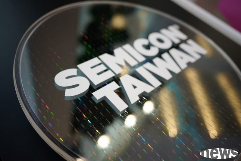
The annual global semiconductor conference SEMICON Taiwan 2025 officially debuted today. As Oracle Cloud End Base Equipment (OCI) will deploy more than 100,000 NVIDIA's latest GPUs in super-centered centralized deployment, providing computing expansion of more than 8 times, and high transmission bandwidth demands have challenged the connection technology structure, making silicon photons (CPOs) a priority for both NTF and NVIDIA.
As the wafer process gradually evolves, the distance between the two signals will affect the transmission of signals, and at the same time increase the transmission consumption. The idea of silicon photon name is to combine the power and light, and to micro-convert the original large optical elements such as couplers and multiplexers into chips, namely photon integral circuits (PICs), and combine the wafers (EICs) into silicon photonic chips.
Before SEMICON Taiwan 2025, Taiwan Chief Huang Shifen shared the current situation of Taiwan’s silicon photonic engine COUPE at the “Silicon Photonic International Forum”, talked about the Taiwan HPC technology platform combining advanced logical chips and high-performance memory (HBM), then added inductors and capacitors, and integrating advanced 3D packaging and silicon photonic solution through advanced 3D packaging.
Huang Shifen demonstrates the silicon photonic platform "COUPE" of teppanel. Its core uses SoIC technology, which represents that EIC (electronic overall circuit) uses copper-to-copper hybrid coupling with PIC (photon overall circuit) circles, integrating all key components within the PIC and an advanced 200G microcontroller (MRM) to complete electrical connection to the substrate.
Enlite Technology also held the "Silicon Photonic Design to Quantity Production: CPO and Different Quality Integration Technology Forum" before the SEMICON Taiwan 2025 meeting, focusing on silicon photons, which are regarded as important technical paths for the next generation. General Manager Su Zhengyu said that the implementation of CPO and Different Quality Integration is not an independent agreement for a single enterprise. Only by connecting the design, process and packaging can we promote the true commercialization of silicon photons.
Su Zhengyu pointed out that silicon photons are regarded as the next main battlefield of semiconductor industry, and integration will be a key. Enlai is committed to building such an integration platform, and using its deep foundation in electronic design automation (EDA), it promotes the implementation of silicon photon design to mass production, and works with partners such as Light Semiconductor and Wave Photonics to provide customers with one-stop solution from design to mass production.
Overall, the legal person stated that it still takes time to introduce silicon photons. Although silicon photon technology has existed for nearly 20 years, due to the slow development of small market size, it has only begun to develop rapidly in recent years, driving short-term internal optical harvesting modules to emit light and heat. However, in terms of standards, optical harvesting modules have standards and agreements compatible with each other. At present, most manufacturers are still improving the standard ordering.